
This is a symbolic initiative to promote cooperation between Japan and South Korea in this industry.
Accordingly, the new facility will cost more than 30 billion yen ($222 million), expected to be located in Yokohama, southwest of Tokyo, which is also the current headquarters of Samsung Research and Development Institute Japan.
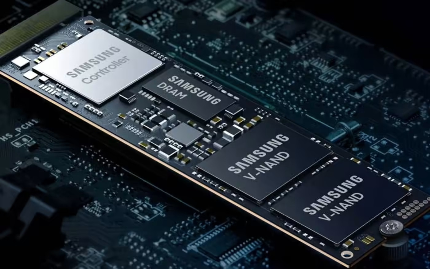
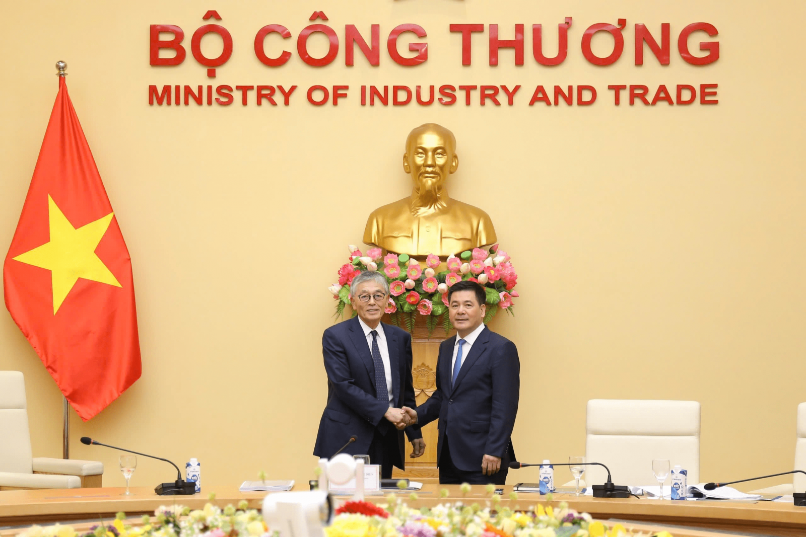
Samsung is the world's largest maker of memory chips, while Japan is a leading producer of basic materials in semiconductors, such as wafers and foundry equipment.
The new facility is targeted to be operational by 2025. Samsung is looking to take advantage of subsidies totaling more than 10 billion yen for the semiconductor sector offered by the Japanese government.
The move by South Korea's most valuable company could spur more cooperation between the two countries' semiconductor industries.
The investment follows a new partnership between Seoul and Tokyo, led by South Korean President Yoon Suk-yeol and Japanese Prime Minister Fumio Kishida. The two leaders are expected to meet on the sidelines of the G7 summit in Hiroshima next week.
Samsung's top rival TSMC also made a major investment in Japan in 2021, diversifying its manufacturing base amid concerns about over-concentration of chip production in Taiwan. TSMC also maintains a research and development facility in Tsukuba, northeast of Tokyo.
Japan, once a global leader in memory chip production, is trying to rebuild its manufacturing base by attracting foreign investment. TSMC and Micron Technology are major foreign investors in Japan and have received government subsidies.
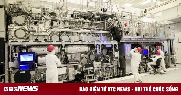
Samsung's new facility will focus on the back-end of semiconductor manufacturing, specifically packaging wafers that have been integrated with circuit boards into final products.
Traditionally, R&D has focused on the early stages of the manufacturing process, aiming to shrink circuits as much as possible. But many believe there is a limit to further miniaturization, and the focus will shift to improving back-end processes, such as stacking semiconductor wafers into multiple layers to create 3D chips.
(According to NikkeiAsia)
Source


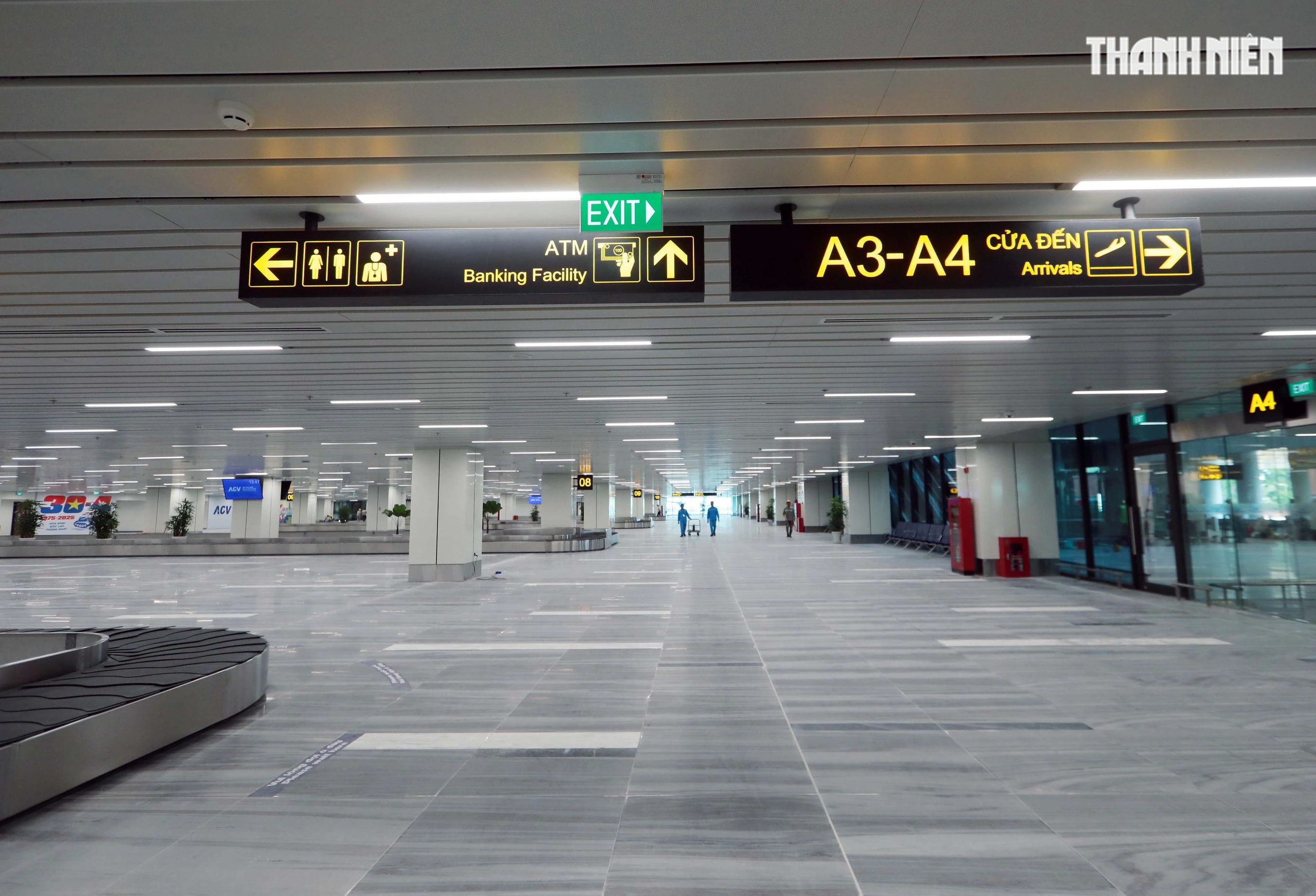
![[UPDATE] April 30th parade rehearsal on Le Duan street in front of Independence Palace](https://vstatic.vietnam.vn/vietnam/resource/IMAGE/2025/4/18/8f2604c6bc5648d4b918bd6867d08396)

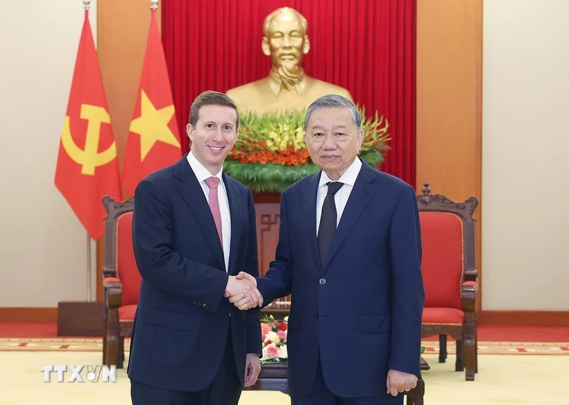
![[Photo] Prime Minister Pham Minh Chinh receives Mr. Jefferey Perlman, CEO of Warburg Pincus Group (USA)](https://vstatic.vietnam.vn/vietnam/resource/IMAGE/2025/4/18/c37781eeb50342f09d8fe6841db2426c)


Comment (0)