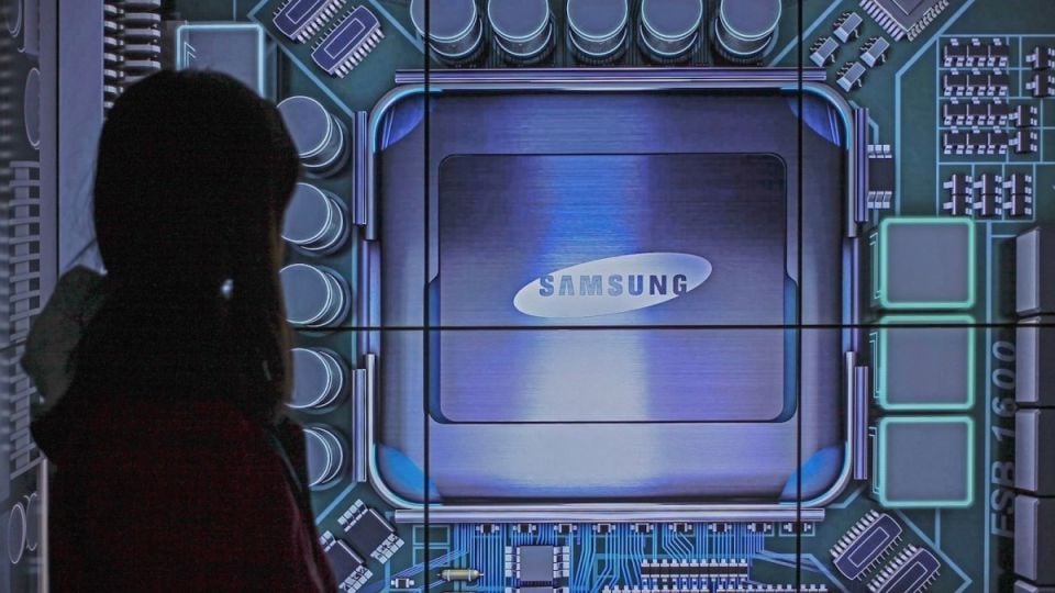
Samsung is the world's largest memory chip maker.
Nikkei Asia reported on May 13 that the cost of building a new chip center in Yokohama, southwest of Tokyo, Japan, is at least 300 million yen ($222 million). This is also where Samsung has a research facility called Samsung R&D Institute Japan. The new center will be built elsewhere in the city.
The investment plan is expected to boost both Japan and South Korea in the chip sector. Samsung is currently the world's largest memory chip maker, while Japan is a leading producer of chipmaking substrates and chipmaking equipment.
There is no specific information about the new investment project yet. It is only known that Samsung will build a production line for prototype chip equipment.
In addition, the new center will focus on the “back-end” stage of the semiconductor manufacturing process, meaning the finished product.
The center is expected to employ hundreds of workers and begin operations in 2025. The South Korean conglomerate is taking advantage of Japanese government subsidies for semiconductor investment.
Samsung declined to comment on the information.
As mentioned above, the move by South Korea's most valuable company is expected to contribute to further cooperation between the two countries' chip industries.
The investment project is a highly symbolic move and follows back-to-back meetings between South Korean President Yoon Suk Yeol and Japanese Prime Minister Fumio Kishida.
Samsung's formidable rival, Taiwan Semiconductor Manufacturing Company (TSMC), has also invested heavily in Japan in 2021. TSMC also maintains a research and development facility in Tsukuba, northeast of Tokyo.
Japan, once the world’s leading chipmaker, is trying to rebuild its domestic chipmaking base by attracting foreign investment. Before Samsung, TSMC and Micron (USA) were among Japan’s major foreign investors and received subsidies from the Tokyo government.
Source link


![[Photo] Readers line up to visit the photo exhibition and receive a special publication commemorating the 135th birthday of President Ho Chi Minh at Nhan Dan Newspaper](https://vphoto.vietnam.vn/thumb/1200x675/vietnam/resource/IMAGE/2025/5/17/85b3197fc6bd43e6a9ee4db15101005b)

![[Photo] Prime Minister Pham Minh Chinh chairs meeting on science and technology development](https://vphoto.vietnam.vn/thumb/1200x675/vietnam/resource/IMAGE/2025/5/17/ae80dd74c384439789b12013c738a045)
![[Photo] More than 17,000 candidates participate in the 2025 SPT Competency Assessment Test of Hanoi National University of Education](https://vphoto.vietnam.vn/thumb/1200x675/vietnam/resource/IMAGE/2025/5/17/e538d9a1636c407cbb211b314e6303fd)
















![[Photo] Nearly 3,000 students moved by stories about soldiers](https://vphoto.vietnam.vn/thumb/1200x675/vietnam/resource/IMAGE/2025/5/17/21da57c8241e42438b423eaa37215e0e)











































Comment (0)